We are influencers and brand affiliates. This post contains affiliate links, most which go to Amazon and are Geo-Affiliate links to nearest Amazon store.
Introduction:
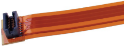
The advent of modern electronic gadgets might not be possible without the flex PCB technology introduction. The flexible PCBs are found in the core of many small and sensitive electronic products. Like camera, smart phones, mobiles, laptops, calculators and other numerous products are using this flex PCB technology.
 The flexible PCB is basically made of a base substrate material from polyimide material. The polyamide/polyimide is a material found naturally and can also be synthetically made to be used in various industries like clothing, automobile and PCB industry. Due to the great flexible nature and high ability to resist heat, polyimide based PCBs i.e Flex PCBs are widely used in electronic equipment where space is minimal and due to small space heat issues can generate. These flex PCBs gives the designer the freedom of mechanical structural designs while assembling the flex circuits inside the enclosure.
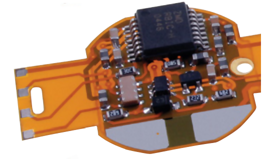
The flex PCBs are mainly / mostly the layers of PCBs embedded / laminated upon each other and components are not soldered upon top or bottom but these flex PCBs works as interconnect or connecting layers or can be replaced with wiring cables. But in various cases we also see that SMT and THT components are soldered on Flex PCBs. The Flex PCBs have good tensile strength and can bear wide temperatures ranges from -200OC to 300OC.
FR4 Rigid Vs Polyimide Flex PCBs
FR-4 base material is the substrate of fiber glass used in rigid (non-flex) PCBs, using the copper cladded pre-impregnated with epoxy resin. The FR-4 gives the mechanical strength to the PCB and has good chemical and thermal conductivity and good electrical insulator, but in some cases where extraordinary heat dissipation is observed like LED light circuits, then other metal or aluminum core PCBs can be used.
Flex PCBs are stable at high temperature, durable and reliable for flexible circuits, chemical resistance is good. The flex PCBs are more costly than FR4 and require extra manufacturing complexity as compared to standard manufacturing process for FR-4 PCBs. A table of comparison between the two is shown below.
| Parameter | Flex (Polyimide) PCB | Rigid (FR-4) PCB |
| Thermal Conductivity | 0.2W/mK | 2.2-2.5 cal./h. cm OC |
| Dielectric Constant @ 1GHz | 4.2 | 4.25-4.55 |
| Dissipation Factor @ 1 GHz | 4.0 | 0.016 |
| Arc Resistance | 143 sec | 125 sec |
| Specific Gravity | 1.6 g/cm3 | 1.8-1.9 g/cm3 |
| Flammability | HB class | UL94-V0 class |
| Electrical strength | 57.1kV/mm | 20 KV/mm |
| Rockwell Hardness (M Scale) | N.A | 110 |
| Compatibility | Special Manufacturing setup | Standard and lead free Assembly |
| Flexural Strength | 340 MPa (50,000 psi) | 415 MPa (60,200 psi) |
Flex PCB (FPCB) Manufacturing Process:
There are numerous types of flexible PCB circuits that can be manufactured at large scale. This complete process takes place in an automated manufacturing facility where conveyer belts and high tech machines carry the fabrication and manufacturing of flex PCB circuits. There are mainly three types of flex PCBs. 1- Single sided flex PCB 2- Double Sided flex PCB 3- Multilayer flex PCB. We will discuss here only double sided PCB manufacturing steps, however multilayer is similar to double sided PCB fabrication just some more internal layers are added but the process remains same. The single sided flex PCB does not have the PTH, electroless plating and pretreatment steps but all steps are same for single sided as for the double sided flex PCB.
 Double Sided Flex PCB Fabrication / Manufacturing:
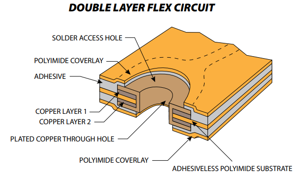
Step-1: The core material for Flex circuits is “Polyimide”. The first step is the cutting of large and very thin polyimide sheets. Automated conveyer machines will carry and delicately cut these sheets in proper panel dimensions as per the design specs. This polyimide sheet is the base material for single sided and inner layers for multilayer PCBs.
Step-2: Thin copper sheet layer is laminated on the base material to be etched and make copper traces and circuit forming. The typical thickness of copper layer used is 0.0007” to 0.0028”. The copper is cladded on the adhesive or adhesive-less base substrate of polyimide.
Step-3: The next step is the chemical cleaning of the panels. These ultrathin panels of flex base material is carefully handled by automatic conveyer belts.
Step-4: Now the circuit is printed on the panel in predetermined board dimensions as found in Gerber files. The photoresist is coated or glued by adhesive on the panel and the circuit pattern or artwork is overlaid on the dry film, now this stack (flex PCB base + photo resist and dry film) is then exposed to UV radiation to “develop” the film. In the case of single sided PCB, only that side that is for component placement will be developed. The dry film can be positive or negative depending on the outer layer or inner layer respectively.
 Step-5: Now the stack will be etched chemically on the same conveyer system and handled very delicately. This will eat away the excess copper and only that copper will remain that is required for traces, pads and holes.
Step-6: Now the drilling will take place on the stack/panel. Ultra small holes are bored using laser drilling and other drills are done by high precision, high speed drilling machines. The blind and buried vias holes are bored for two sided or multilayer PCB panels.
Step-7: At this stage now is the time for copper plating. The electroless copper is done and very thin layer of copper is chemically deposited on the walls of the through holes bored in the previous step. Now after electroless copper plating, the electroplating is done for the entire panel where thick layer of copper is deposited electrically on the walls of PTH (plated through hole).
Step-8: The next step will be the pre-treatment. Because of the contamination due to various factors like chemicals, ink or adhesives the oxide layer can be formed on the surface. Hence the panel surface is pre-treated with cleaning agents like alkaline or panel can be brushed with abrasive.
Step-9: Now the polyimide coverlay is placed over the exposed conductors using epoxy or acrylic adhesives. The photoimgeable coverlay are also used for HDI (High density interconnect) PCBs but may not be as resilient as polyimide.
Step-10: Now the surface finish is done by ENIG or HASL process.
Step-11: Now the stiffeners are applied to the final stack to give additional rigidity to the specific areas of flex PCB where strain relief components are to be installed in assembly to give mechanical firmness.
Step-12: At this step your flex PCB is complete. It is time now to perform electrical test based on net list of the circuit and PCB layout as provided by the designer. Voltage, current, impedance test are performed and final inspection for shorts, open, bridges and other possible anomalies are identified. Grid test and flying probe test can be done.
Step-13: Outlining, cutting and V-scoring is done in the final step. The multiple boards are cut out from the panel by means of punch and die. V-Groove cutting or scoring is done. Outlining can be done by laser cutting.
Step-14: Now the final QC, packing and shipment is done to deliver the PCBs to their end customers/users.
We are influencers and brand affiliates. This post contains affiliate links, most which go to Amazon and are Geo-Affiliate links to nearest Amazon store.
I am interested in all things technology, especially automation, robotics and tech that helps change how society will live in the future.

